The HP 9825A/B calculators will have one or two read / write memory boards. The 9825 having only one, base R/W Memory board, will have a dummy board in top R/W Memory board position.
The 16 kB of R/W Memory base board is based on 32x DRAM TMS 4060 chips, each 4096 x 1bits. The rest of circuitry on the board controls the refreshing, byte operations, write enabling and address recognition. I have also 8 kB R/W Memory base board.
The memory area of the R/W Memory base board starts at address 7FFFH down. To 7D68H is a stolen R/W area, not available for users. It is used for temporary storages of variables by the system firmware for its internal operation. The end address of 16 kB R/W Memory base board is 6000H and 7000H if only 8 kB R/W Memory base board is installed.
I have created full documentation for the memory boards with schematics, PCB layout, Gerber and Excellon files.
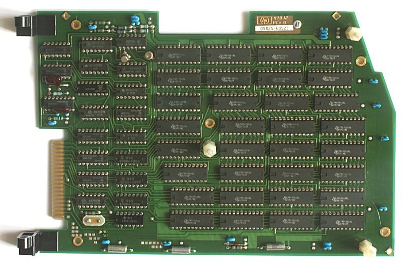 Fig. 1 - original board 9825A-69523 Memory board
Documents:
schematics
components location on PCB
bill of materials (BOM)
connector signals pinout

