The HP 9825A/B calculators will have one or two read / write memory boards. The 9825 having only one, base R/W Memory board, will have a dummy board in top R/W Memory board position.
The 8 kB R/W Memory option board is based on 16x DRAM TMS 4060 chips, each 4096 x 1bits. Full board has memory of 8192 bytes. Installation this option 8 kB R/W Memory allows to use Extended I/O ROM, Advanced Programming ROM and String ROM. The System Programming ROM needs 32 KB model of R/W memory.
The memory area of the R/W Memory option board starts at address 5FFFH down. The lowest R/W Memory address is 4000H. However from 4000H to 4FFFH is an address conflict with Option ROMs. If HP 9825 has 32 kB R/W Memory (16 kB base + 16 kB option R/W Memory), it cannot use Strings, Extended I/O or Advanced Programming ROMs. Conversely, if HP 9825 uses any or all of these ROMs, it cannot operate with two 16 kB R/W Memory boards. This address conflict cannot be eliminated with switches on CPU board
I have created full documentation for this memory option board with schematics, PCB layout, Gerber and Excellon files.
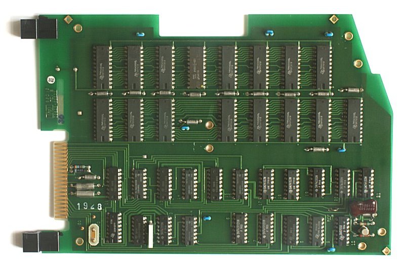 Fig. 1 - original board 9825A-69522 Memory Option Board
Documents:
schematics
components location on PCB
bill of materials (BOM)
connector signals pinout

